

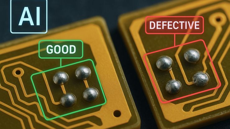
AI Image Analysis for Reliable Defect Detection
AI-based visual inspection with microscopy helps make quality control in industrial environments efficient by reducing manual inspection effort concerning defect detection, classification, and…

An Overview of Artificial Intelligence (AI) and Machine Learning
AI is rapidly changing industrial inspection, quality control, and manufacturing workflows. But not all AI technologies work the same way. From machine learning and deep learning to the newer concept…
Why the Future of Microscopic Inspection Is AI-Assisted, Not Fully Automated
The next wave of QC productivity gains will not come from building more automated inspection lines. Instead, it will come from augmenting millions of inspection decisions that are made manually every…
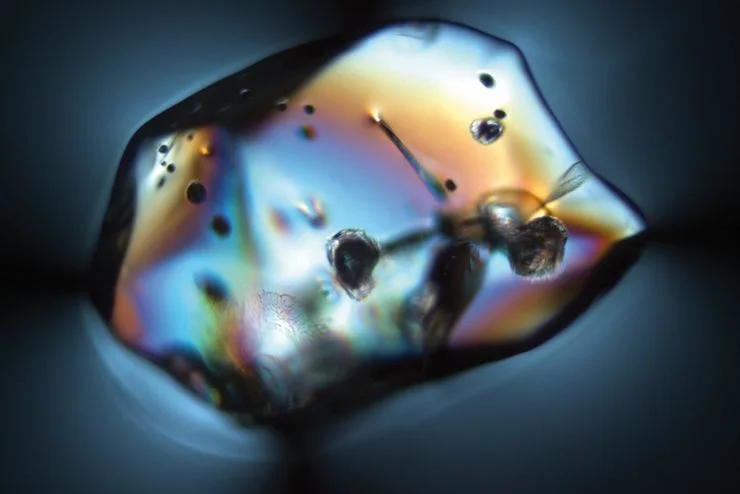
利用偏光显微镜优势确保玻璃质量
玻璃是已知最古老的材料之一。如今,玻璃被广泛应用于各种领域,如光学仪器、门窗、太阳能电池板、食品、饮料和药品容器等,因此必须符合严格的玻璃质量标准,尤其是光学玻璃。利用偏光显微镜对平板玻璃、中空玻璃和压制玻璃进行质量控制既快捷又经济。无需进行耗时的样品制备,即可对结节、金属、晶体夹杂物和气泡等缺陷进行分析。
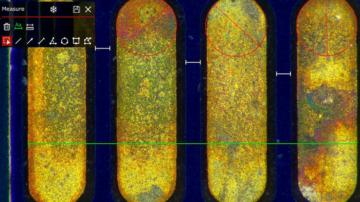
如何选择合适的测量显微镜
使用测量显微镜,用户可以测量样品特征的二维和三维尺寸,这对检测、质量控制、故障分析和研发&D 至关重要。然而,选择合适的显微镜需要评估应用需求以及显微镜的性能、易用性和灵活性。 如今,测量通常以数字方式进行,即使用带有摄像头和软件的显微镜,图像显示在显示器上,而不是通过目镜网线,从而提高了精度和可重复性。使用合适的测量显微镜可靠、快速地分析样品。
显微镜测量校准:为什么要这样做?
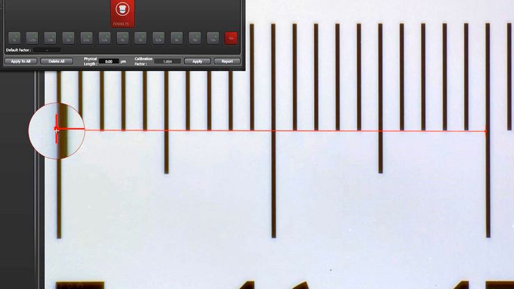
显微镜校准可确保检测、质量控制 (QC)、故障分析和研发 (R&D) 所需的测量准确一致。本文介绍了校准步骤。使用参照物进行校准可使结果具有可重复性,并有助于确保与准则和标准一致。为了获得准确一致的结果,建议校准显微镜并定期检查。如有需要,可向校准专家寻求支持。
晶圆表面光刻胶残留与有机污染物可视化检测
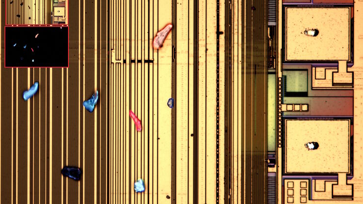
随着半导体集成电路 (IC) 的尺寸缩小到 10 纳米以下,在晶圆检测过程中有效检测光刻胶残留物等有机污染物和缺陷变得越来越重要。光学显微镜仍是常用的检测方法,但对于有机污染而言,明视野和其他类型的照明都有其局限性。本文讨论了在半导体行业的质量控制、故障分析和研发&D 过程中,如何利用荧光显微镜有效检测晶片上的光刻胶残留物和其他有机污染物。
Rapidly Visualizing Magnetic Domains in Steel with Kerr Microscopy
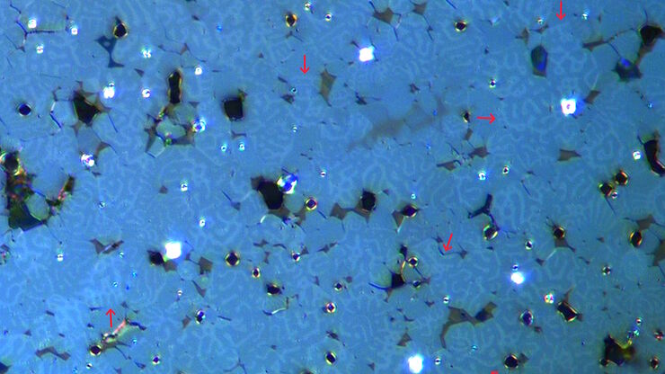
The rotation of polarized light after interaction with magnetic domains in a material, known as the Kerr effect, enables the investigation of magnetized samples with Kerr microscopy. It allows rapid…

6 英寸晶片检测显微镜,可靠的观察微小高度差
本文介绍了一种 6 英寸晶圆检测显微镜,无论用户的技术水平如何,它都能自动进行可重复的 DIC(微分干涉对比)成像。集成电路 (IC) 芯片和半导体元件的制造需要晶圆检测,以确保不存在影响性能的缺陷。通常使用光学显微镜进行质量控制、故障分析和 R&D 检测。为了有效地观察晶圆上结构之间的微小高度差,可以使用 DIC。


