
Filter articles
标签
Loading...

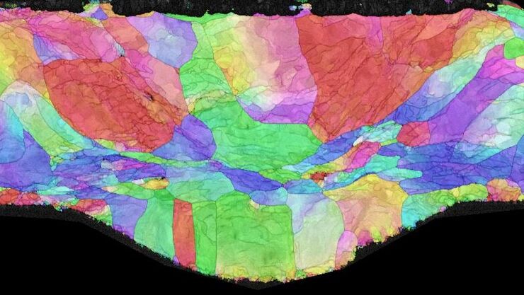
偏振光显微镜影像图集
偏振光显微镜(又称为偏光显微镜)是一种应用于不同领域的重要方法,包括研究和质量保证。它不仅仅是在高倍率和高分辨率下产生图像,这通常是用普通光学显微镜完成的。
通过检查样本的形状、结构、颜色、双折射和进一步的光学性质,可以获得有关样本结构、光学性质和成分的附加信息。
Loading...

验证汽车零部件的规格
在汽车零部件的开发和生产过程中,无论是供应商还是汽车制造商,都必须符合规格要求。这些规格对保持汽车和其他车辆在生命周期内的性能标准和安全运行至关重要[1,2,3]。在满足或超越日益严格的质量标准的同时,对更高效和更具成本效益的零部件开发和生产的需求一直在提高。本文解释了如何用数码显微镜轻松快速地研究和记录零件以确定其是否符合规格要求。
Loading...

偏振光显微观察
偏光显微镜通常应用于材料科学和地质学领域,根据矿物的折射特性和颜色来识别矿物。在生物学中,偏光显微镜通常用于晶体等双折射结构的识别或成像,或用于植物细胞壁中纤维素和淀粉粒的成像。

Loading...

高效清洁度分析的关键因素
在汽车和电子行业,零部件上细小的污染颗粒物也可能影响产品的性能,导致产品出现故障,或使用寿命缩短。对于汽车来说,过滤系统很容易受到影响。对于电子产品来说,印刷电路板(PCB)或连接器上的污染可能会导致短路。因此,清洁度在现代制造业的质量控制中占有核心地位,特别是使用由不同供应商生产的部件时,更要重点关注清洁情况。车辆或设备的关键部件如果受到污染,整个系统就可能发生故障。因此,高效清洁度分析过程必须…

 and oblique (right) brightfield illumination using a Leica compound microscope. The defect on the wafer surface is clearly more visible with oblique illuminati")
Loading...

电子产品制造截面分析
本文将讨论印刷电路板 (PCB) 和总成 (PCBA)、集成电路 (IC) 和电池组件的横截面为什么对质量控制 (QC)、故障分析 (FA) 和研发 (R&D) 有效,以及如何制备这些横截面。
