. With DIC users are able to visualize small height differences on the wafer surface more easily.")
简介
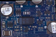
半导体元件生产过程中的晶圆检测对于识别和减少可能影响元件性能的缺陷至关重要。为了提高检测精度和效率,光学显微镜解决方案应结合不同的对比方法,提供有关图案晶片上可能存在的任何缺陷的准确可靠信息。在晶片检测中发挥重要作用的一种对比方法是微分干涉对比法(DIC)。
什么是 DIC?
微分干涉对比(DIC)又称诺马斯基对比,有助于观察样品表面的高度差异 [1,2]。DIC 使用沃拉斯顿棱镜、偏振镜和分析仪(参见图 1A)。偏振器和分析仪的偏振平面相互垂直(交叉 90°)。通过棱镜的偏振光会被剪切成两个偏振相差 90° 的波。离开棱镜后
然后,这两束光波从样品表面反射并返回物镜。由于样品表面的形态或光学特性不同,光线可能会经历不同的光路长度,从而导致一条光线与另一条光线相比产生相位偏移。光线穿过物镜棱镜和分析仪后,会重新组合成一条光线,然后它们之间会发生干涉。DIC 图像显示出强度和颜色的变化,从而呈现出纹理的外观。DIC 可使高度差异一目了然,而其他类型的照明(如明视场或暗视场)通常无法做到这一点。有关 DIC 的更多信息,请参阅参考文献 1 和 2。
下图 1 举例说明了与明视野和暗视野照明相比,DIC 如何增强样品表面的高度差。使用 DIC 对图案晶片样本进行成像。使用 DIC 时,样品元素之间的高度差更加明显。

使用 DIC 时面临的挑战
DIC 使用户能够直观地看到晶圆上结构之间的微小高度差,但对许多用户来说,使用起来可能比较复杂。正确调整 DIC 棱镜对于获得最佳对比度和准确、可重复的结果至关重要。例如,DIC 图像中样品结构的垂直方向(进入或离开样品水平面)在很大程度上取决于棱镜对光波的剪切。
因此,剪切会影响结构之间的高度差,即图像中的一个结构看起来比另一个结构高或低。剪切通常显示为正偏差或负偏差(参见下图 2),但偏差通常与实际高度差不相关。对于大多数光学显微镜来说,除了偏振镜和分析仪的交叉外,还需要手动调节 DIC 棱镜。不过,用户应具备丰富的经验,以获得可比、一致的 DIC 结果。要获得 DIC 对比度非常好的图像,用户需要花费大量的时间和精力进行手动调整。
 拍摄的 图案化晶圆区域图像。")
自动和可重复 DIC 成像的优势
对于手动 DIC 操作,显微镜照明和对比度设置的调整必须始终由用户直接完成。图像效果在很大程度上取决于用户的经验和技术水平。然而,通过提供自动 DIC 操作的显微镜,可以实现用于质量控制、故障分析和 R&D 的高效晶片检测工作流程。即使是经验不足的用户,也只需对设置进行少量更改,就能轻松完成可重复的 DIC 成像。只需按下按钮,就能选择合适的棱镜,并根据入射光波的剪切效果调整棱镜的位置,而且设置会自动存储,方便调用。在使用 DIC 时,这一功能也是可靠记录的关键。
具有可重现 DIC 的 Leica 解决方案
使用 DM6 M 显微镜可以对 6 英寸晶片进行快速、可靠的检测(参见图 3)。它可对晶片和半导体元件进行自动和可重复的 DIC,这要归功于以下功能:
- 专为 6 英寸晶片设计的平台
- 最佳交叉偏振器和分析器(称为 ICR 立方体)
- 通过棱镜的电动和编码定位,调用精确的 DIC 设置
- 专用 DIC 棱镜和 ICR 立方体带来均匀对比度
- 由于采用了自动显微操作,可自动选择和调整正确的棱镜和 ICR 立方体,因此使用简单快捷。
DM6 M 比用于晶片检测的典型显微镜占地面积更小,因此还能节省工作区的空间。

成像 对图案化晶圆的不同区域进行观察,光波剪切分别采用 负偏置(A 和 C) 和 正偏置(B 和 D)。")
明场照明 和 B)暗场照明 进行成像。")

 and oblique (right) brightfield illumination using a Leica compound microscope. The defect on the wafer surface is clearly more visible with oblique illuminati")